
Building a clone of the original Pong game board
Atari's PONG is probably one of the oldest widely known videogame in history. Prior to this, other digital video games existed, but none were so well executed. It was a huge commercial success.
What's more amazing about this game, is that it was designed and created before microcontrollers existed. And therefore everything is made using discrete logic components. This means there was no software, no reprogramming and no easy way to fix the bugs.
It was also made long before the CAD and simulation tools we use today. So everything had to be designed by hand, carefully calculating and testing every step.
I also think this board has great educational value for people learning discrete logic electronics, and that's why I decided to recreate it myself, with a few modifications.
Part 1: Research
Of course I had absolutely no clue on how to even start so I began searching the web for posible resources. The first thing I encountered was a couple of high resolution images of other board clones, with one of them even showing both sides:


As we can see, it's composed mostly of DIP14 and DIP16 ICs, organized in columns which vary depending on the clone. On the right side is the non-logic part of the board, composed mainly of input power and output video and audio and other things I've yet to discover. On the top right there seems to be a voltage regulator attached to a heatsink which is also attached to the main board traces to dissipate the heat. There also seems to be an big capacitor right after this transformer maybe to avoid fluctuations in the power supply.
The two main traces are the power traces which are usually thicker than traces carrying logic signals. Power is distributed through all the columns, having each column a ceramic or polyester film capacitor acting as decoupling capacitors to avoid brownout of the ICs.
These kind of capacitors are normally recommended to be placed as near as possible to the VCC/GND pins of ICs to ensure no tx-line effects affect the supply of power. However in this situation it seems the designers decided to let the ICs share the decoupling capacitors with some exceptions here and there.
There's also a switch in the middle of the board which I have no clue what it does.
If we observe the logic-signal traces, they seem to have been routed manually one by one. The traces on the top layer are oriented vertically and horizontally on the bottom layer. This is usually considered a good practice as if they were oriented in the same direction they would interfere with eachother, adding noise to the logic signal. Also, there's barely any room in the top layer for the traces to move because all ICs are surrounded by the power traces.
Okay enough analysis of the image. I was also able to find the original board topology and circuit diagram of the board:


As we can see the board is made only using the 74xx family of logic ICs (and 555 timers). The schematic has been divided into sections which show the function of each block. (A lot later I found the full original document here.)
Even though the previous images are somewhat useful, the text was quite blurry and I wasn't able to read all the components and connections. So I kept searching...until I found the two most useful documents.
- The first one was a very thorough analysis of the board logic performed by Dr. Hugo Holden and titled ATARI PONG E CIRCUIT ANALYSIS & LAWN TENNIS:BUILDING A DIGITAL VIDEO GAME WITH 74 SERIES TTL
- The second one was a complete redraw of the original schematic performed by Dan Boris.
This was what I needed to get started.
Part 2: Redrawing the schematic in Altium Designer.
Note: If you don't want the whole circuit explanation, you can skip to Part 3 (waaay below) in which I make the PCB.
Using Dan Boris's schematics as a reference I was able to recreate most of the schematics. However, just as Pong74Is pointed out, some of the logic chips have become obsolete and had to be replaced with newer parts which performed the same function but had different pin connections. Some other components weren't even sold in my country and therefore I tried to replace them with a combination of other components.
I'll attempt to describe each part of the new design just as Dr Holden did, but showing the updated/modern schematics.
POWER
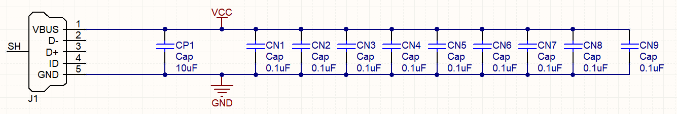
Pretty straightforward stuff. I decided the board would be powered via USB port, instead of the original slot. I think think this way it would be easier to just plug it in everywhere instead of having to carry around a transformer, etc.
There's a main cap (CP1) to maintain steady voltage globally. These caps are normally very slow, so they can't react to quick changes in voltage. For this I've added the capacitors CNn which, like in the original design, will be used as decoupling capacitors in each row of ICs in order to avoid brownout caused by the fast switching. The kind of capacitors normally used for this are small valued ceramic capacitors, which react faster than the large electrolytic ones.
CLK
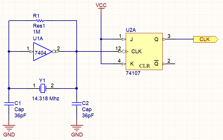
This is the heart of the whole circuit. A Pierce Oscillator feeding a JK Flip-Flop which is set in Toggle Mode. This means the Q signal will toggle on every cycle of the original clock, dividing it once. This JK Flip-Flop is also acting as a buffer to the original clock as the circuits to make clocks are normally very sensitive and have a low current capacity (low output impedance).
The original schematic used another kind of oscillator and a NAND gate to buffer the signal, but I think this configuration might work.
As we can see, the crystal used is 14.318 Mhz, which is the standard crystal used for NTSC video (the reason for this value came from the color burst frequency after color was added to NTSC TV...but we don't care about that as we are only going to use Monochrome NTSC). If you don't know anything about composite video, you can checkout batsocks article which explains how everything works.
The CLK signal will therefore be 7.159 Mhz. This is the clock which will feed the rest of the circuit.
The tables below show the amount of cycles to count to produce the official NTSC timings.
Table: NTSC Horizontal Timings
| Period (us) | Cycles | Cycles Approx | |
|---|---|---|---|
| Active Video | 52.6 | 376.6 | 337 |
| Front Porch | 1.5 | 10.7 | 11 |
| Sync Pulse | 4.7 | 33.6 | 34 |
| Back Porch | 4.7 | 33.6 | 34 |
| Full Horizontal Line | 63.5 | 454.6 | 455 |
Table: NTSC Vertical Timings
| Period (us) | Lines | Lines Approx | |
|---|---|---|---|
| Active Video | 15335.25 | 241.5 | 242 |
| Front Porch | 190.5 | 3 | 3 |
| Sync Pulse | 190.5 | 3 | 3 |
| Back Porch | 762 | 12 | 12 |
| Full Frame | 33337.5 | 525 | 525 |
However, because the original designers wanted to reduce the amount of wiring and connections, they prioritized using less logic gates. These logic gates are the ones which combine the signals from the clock dividers to get the actual count.
Therefore, they could only use powers of two as cycle counts in their signal timings, so they ended up choosing the powers of two which approximated as closely as possible to the actual timings:
Table: Pong Horizontal Timings
| Cycles | Period (us) | |
|---|---|---|
| Active Video | 375 | 52.38 |
| Front Porch | 32 | 4.47 |
| Sync Pulse | 32 | 4.47 |
| Back Porch | 32 | 2.23 |
| Full Horizontal Line | 455 | 63.56 |
Table: Pong Vertical Timings
| Lines | Period (us) | |
|---|---|---|
| Active Video | 246 | 15634.67 |
| Front Porch | 4 | 254.22 |
| Sync Pulse | 4 | 254.22 |
| Back Porch | 8 | 508.44 |
| Full Frame | 524 | ? |
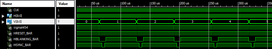
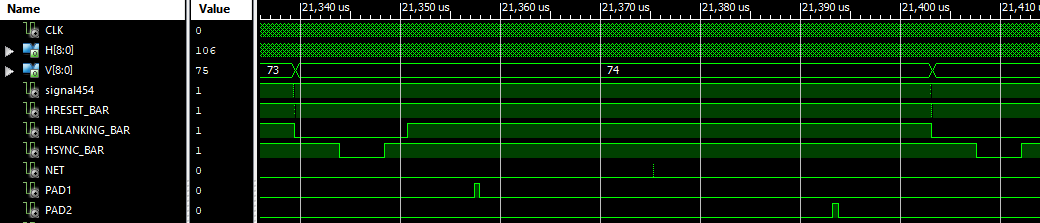
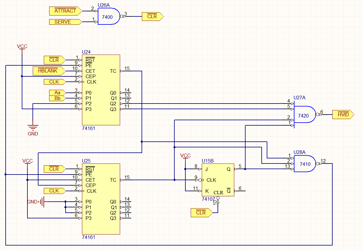
HSYNC
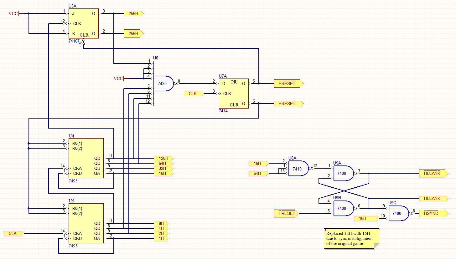
Each 74161 IC contains 4 flip-flops, each dividing the frequency of the clock by half. So the 1H signal will contain CLK/2, 2H will contain CLK/4, and so on...
This way, each flip-flop is able to count up to 15 in binary with a frequency of CLK. If we wish to count higher, we could connect the output of the signal with lowest frequency to the clk entrance of the next flip-flop as what's called a ripple counter.
Using the whole 9 flip flops included in the 7493 and the 74107, we're able to count up to 511!
In order to trigger something on a specific count, we use a NAND gate (7430) which will go LOW when all of it's inputs go HIGH. This means that if we connect the 256H, 128H, 64H, 4H and 2H signals, the output of the NAND will get LOW when the count is 256+128+64+4+2 = 454. This allows the 7474 Flip Flop to get triggered on the next cycle, making the HRESET signal LOW after 455 cycles and resetting all the counters. This is the amount of cycles we previously specified on our table as the length of a line in the TV.
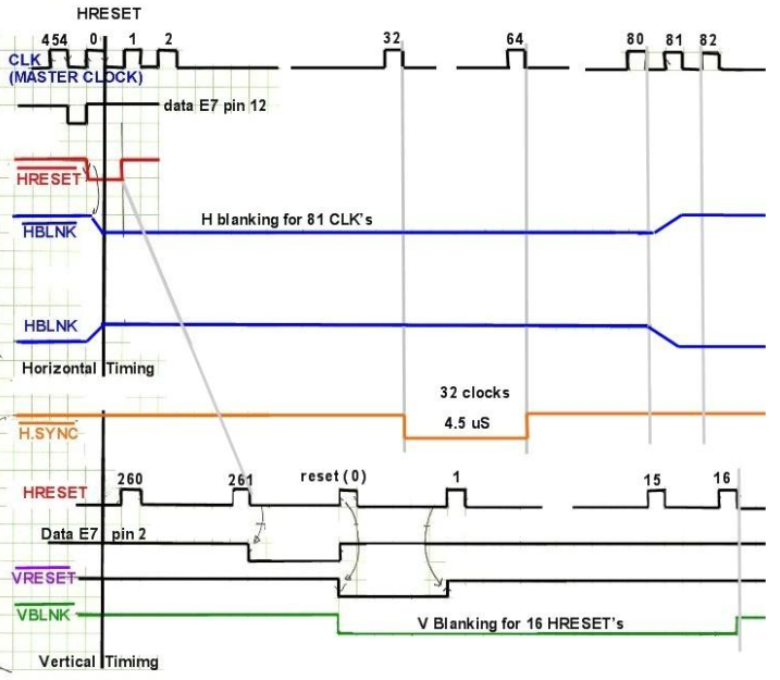
The 64H and 16H pulses and the HRESET pulse are used to create the HBLANK and ~HBLANK (Horizontal Blanking and not Horizontal Blanking) and 32H pulses are used to create the ~HSYNC (not Horizontal synchronising pulses)
The two parallel 7400 NAND gates act as a negative edge S-R Latch, where HBLANK will get HIGH when the count is 80 (64H+16H), and will get LOW when HRESET is LOW. Which means HBLANK will be LOW from 0 to 80, and then it will be HIGH from 81 to 455.
The ~HSYNC signal is the intersection of the ~HBLANK signal and the 16H signal. Which means ~HSYNC will be LOW from 16 to 31, only when ~HBLANK is LOW.
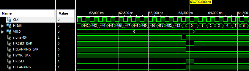
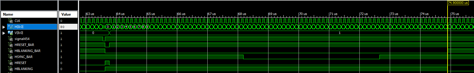
If you were not able to follow along all the way, here's an image from Dr. Holden's document, along a simulation I made in Verilog:
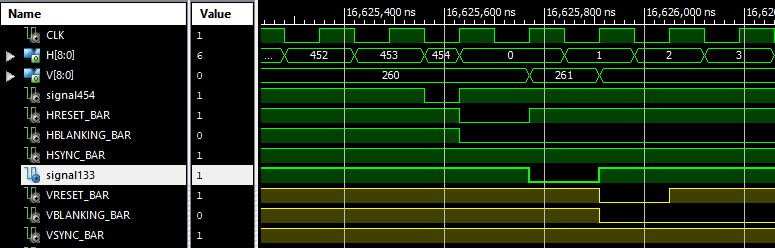
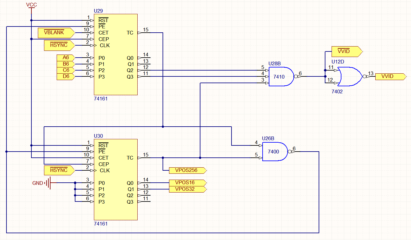
VSYNC
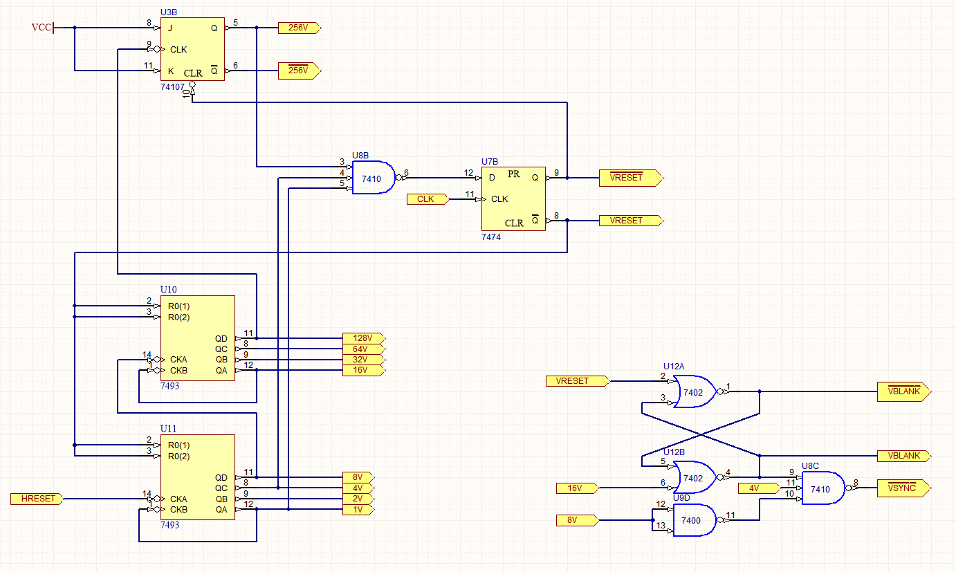
This part is very similar to the HSYNC one, but this time, the counters are fed with the HRESET signal as a clock instead of CLK signal. This way the HRESET signal acts as a line counter for the frame.
The amount of lines we wish to count is 262, which is the amount of lines in a field (half a frame in interlaced NTSC). So as before we use the NAND gate to combine 256+4+1 = 261, plus the cycle the D Flip-Flop adds.
The VBLANK and VSYNC part also acts in a simliar way as the previous figure, but this time it's a NOR S-R Latch, which means it's postively triggered: when VRESET goes HIGH, VBLANK goes HIGH, and when the count is 16, ~VBLANK goes LOW.
~VSYNC is the intersection of VBLANK, 4V, and 8V, which means ~VSYNC will be LOW from 12 to 15, only when also VBLANK is HIGH.
Now that we have the basic NTSC video functionality, we can start drawing stuff on the screen!
Just in case you have forgotten how the game looks, i'll leave a screenshot of it, this will aid us in the future sections:

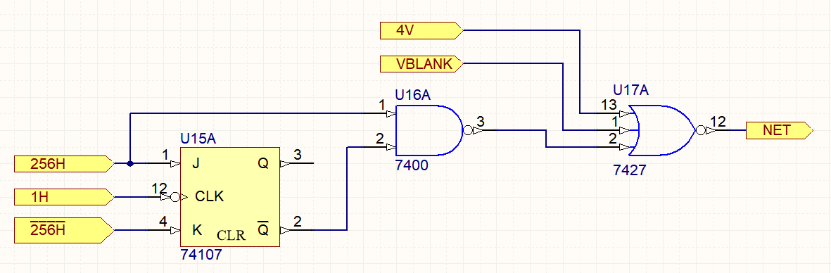
The net consists of a dashed line in the "center" of the screen, each dash is 4 lines tall (separated by 4 lines), with a thickness of 1 cycle/"pixel".
We use a gate circuit so we can generate gated pulse for drawing the net. In this case, the J-K Flop-Flop is acting as a D Flip-Flop, which on each 1H cycle clocks the 256H signal to Q. So assuming 256H is LOW, on each cycle ~Q will have HIGH, and therefore the output of the NAND gate will be HIGH. When 256H changes to HIGH, the NAND will instantly have HIGH in both of its inputs and will output LOW. After that, 256H gets clocked to ~Q, which will now be LOW, and therefore the output of the NAND will again be HIGH.
This way we obtain a single negative pulse at the output of the NAND, when the count is 256, which is about "half" of a line length (the net will get drawn at the "center" of the screen.)
In other words, we're positioning a pulse (the net) at 256H with a duration (thickness) of 1H.
This signal then gets NOR'd with VBLANK and 4V so that the Net only gets drawn every 4 lines, and when the screen isn't blanking.
Paddles
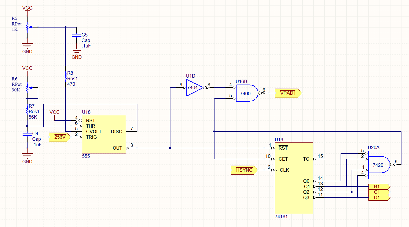
The paddles are 4 sync pulses/"pixels" thick and and 15 lines tall. The circuit for both paddles are exactly the same, the only difference is it's horizontal position.
The way it works is by using a potentiomenter, a 555 timer and a 4 bit counter.
When ~256V falls LOW at the beginning of vertical blanking, it triggers a 555 timer. This creates some delay depending on the position of the player's 1K potentiometer connected across the 5 volt supply and to the 470 ohm resistor connected to pin 5 of the 555 timer IC (this pin modulates the width of the 555 timer pulse within the 1.1*RC period).
When the 555 timing period ends, the reset pin in the 74161 falls LOW and starts to count horizontal sync pulses.
(In the original schematics they used a 7493 IC. But I've decided to try to replace it with a 74161.
Also, at the start of this count ~VPAD1 goes low. The counter counts up to 15 and at that time the output of the 4-input NAND goes LOW. This causes ~VPAD1 to go high and also stops the count leaving the counter full.
Effectively 15 lines are counted, starting at some point on the scan after a player controlled delay from the start of the vertical blanking interval.
When the 555 is retriggered from the ~256V the next time around and pin 3 of the 555 goes high again, the outputs of the 74161 get reset (zeroed) and the process repeats.
The least significant bit, from the counter’s Q0 output is not used. The binary values of the B1, C1 & D1 outputs are ultimately encoded to a range of new values in the vertical velocity encoder
The second paddle is exactly the same as the first one.
In the lower part of the figure above is the part which determines the positioning and thickness of the paddles.
Just like in the net part, there's a gated pulse happening at the D Flip-Flop, which should position the paddles at 128 and 384.
However, because this signal is combined with the 256H + VPAD1 and ~256H + VPAD2 at the NORs, it gets filtered to the left half of the screen (with the 256H) forming the left paddle PAD1, and to the right side of the screen (with ~256H), forming the right paddle PAD2.
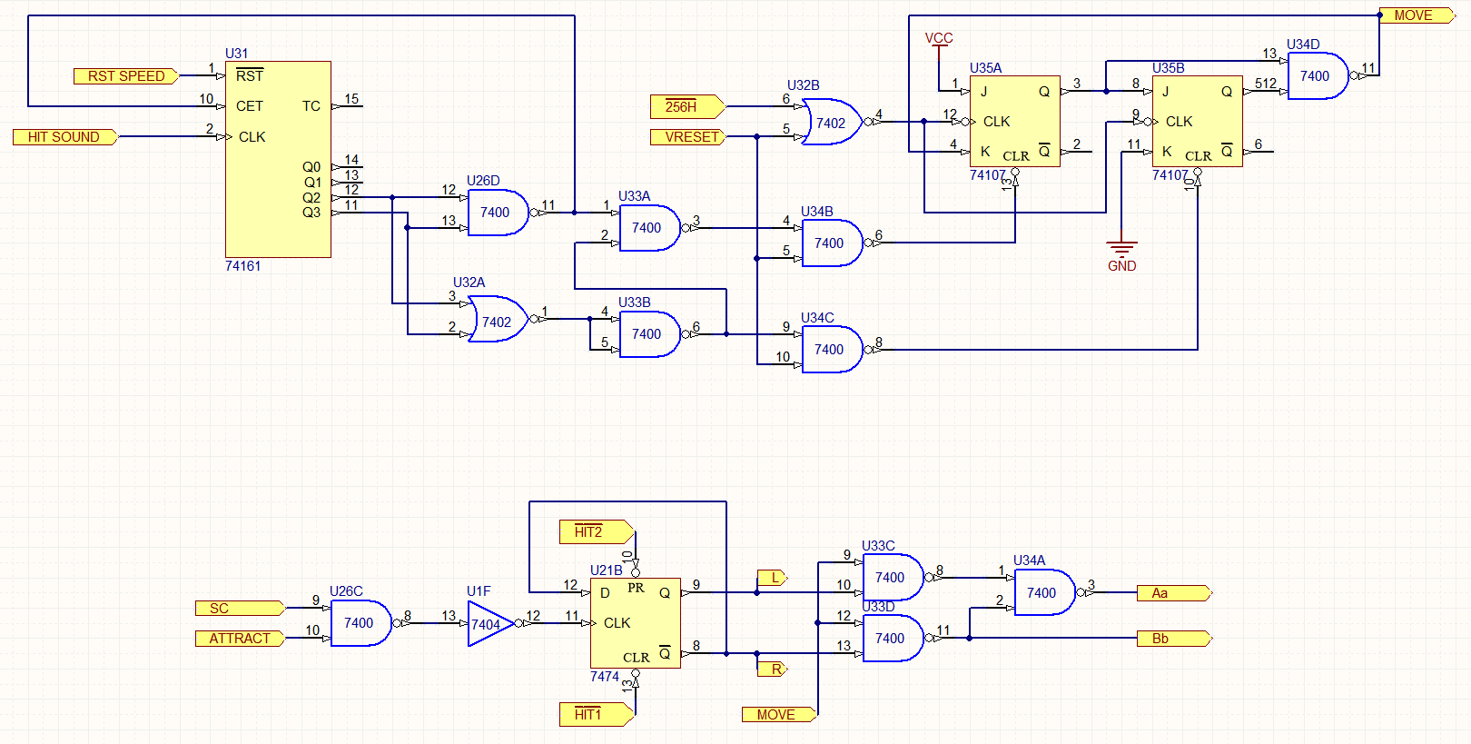
Ball
In order to render de ball, the board uses an identical sets of counters as in the HSYNC and VSYNC part. These counters, however, only count while in active video, beacuse they get suspended by HBLANK and VBLANK
This way, if the HSYNC counter and the HVID counter are in sync, the ball won't move in the horizontal direction. Same applies for the VSYNC counter, VVID counter and vertical direction.
The ball, then, will move when both counters are out of sync, as the ball rendering signal will get rendered before or after it should (signal will arrive early or delayed with respect to the sync signal).
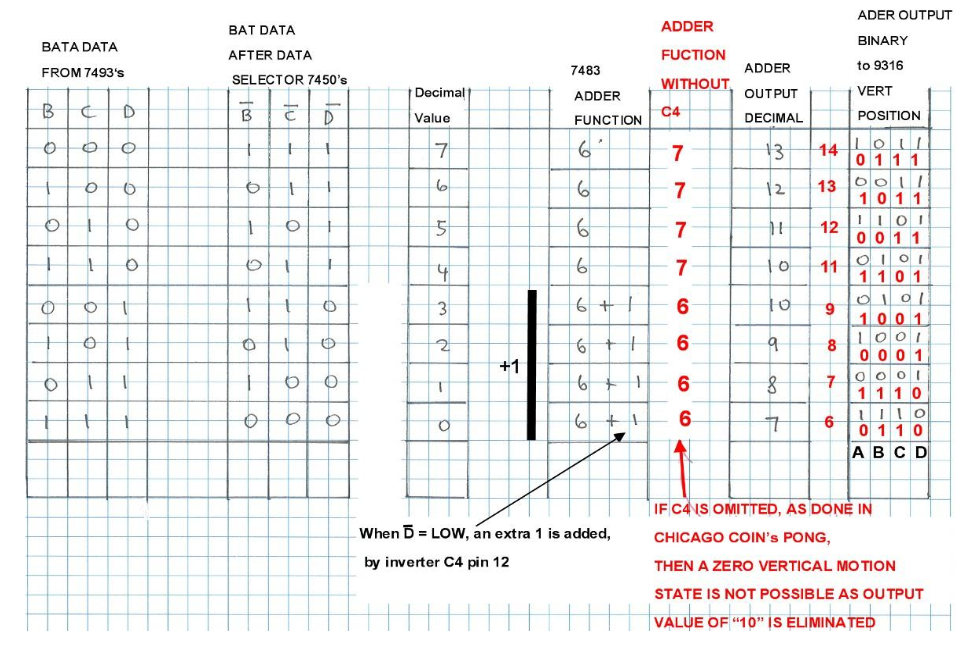
The Aa, Bb, A6, B6, C6 and D6 are the values loaded as initial values for the counters, and they represent the following:
In the case of horizontal motion, the two counters combined can count up to 255 (this is when the two TC signals get triggered). When this happens the JK flip flop gets toggled in the 256th clock cycle.
If we assume the output of this flip flop was LOW before it toggled, the NAND gate won't get triggered until the next time the counters are full. In other words, before triggering the NAND which loads initial values to the counter again, the counter has to get filled twice: the first time it toggles the flip flop, and the second one activates the NAND.
If we load, for example the number 2 into the counter (through Aa and Bb, which means there shouldn't be any horizontal motion), the first counter will actually get loaded with 8+2=10, while the second one will get loaded with 128.
The full counter, then, starts counting from 128+8+2 = 138. Which means that in order to fill the full counter, it has to count 255-138 = 117 cycles. This is what happens the first time the full counter gets filled, when the JK flip flop toggles.
In the next clock cycle (118) the counters overflow and start counting again for a second time. This time, the counters count from 0 and therefore count 255 cycles.
This means the grand total counted by the counters when the NAND activates is 255+118 = 373.
But wait! The loading of the initial values also takes one clock cycle. So in the 374th cycle, the counters load Aa and Bb again starting the whole cycle again.
This means the horizontal rendering of the ball is in sync with the number of cycles in Active Video, and therefore the ball shouldn't move (remember, this only happens because we loaded a 2 into the counter).
In the case of vertical motion, if we load the number 10 to the first counter, it will count 245 lines until both counters are full. When this happens, the new values waiting to be loaded (A6-D6) are loaded into the counter. This action takes 1 extra clock cycle, so from the moment the counters are full to the next time the counters are full, 246 cycles/lines are counted. Which is exactly the amount of lines in Active Video, and therefore the ball won't move vertically.
The VVID signal which renders the vertical component of the ball is active from 255+8+4 = 267 to 255+16 = 271 (or 257 to 261 if 10 was loaded), which means it's active for 4 cycles giving a height of 4 lines.
Ball Position Encoding
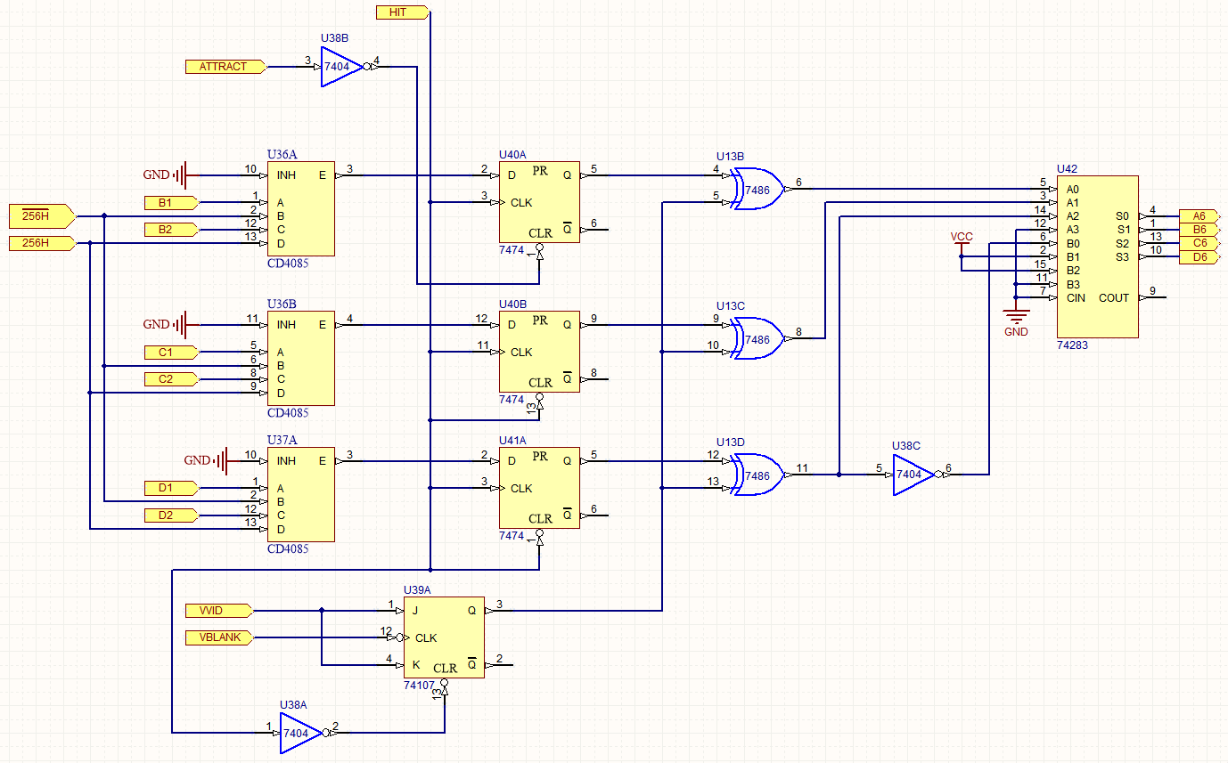
Each time the ball hits a paddle, it gets a different vertical velocity depending on which part of the paddle it hit. The closer it hits to the edges, the greater the vertical velocity. That means if the ball hits the paddle exactly in the middle, it will have no vertical velocity and therefore the ball will bounce pefectly perpendicular to the paddle
The vertical velocity also gets reversed/inverted when it hits the top and bottom edges of the screen
The B1, B2, C1, C2, D1, D2 encode the vertical velocity which will get loaded into the "vertical velocity register" of the ball
In the left part (7408 + 7402) is the data selector. Just as in the previous section, ~256H selects the left side of the screen image and 256H the right so this is how each players bat is selected from two identical player bat data circuits.
The 3 bit bat data is inverted by the outputs of the NORs and is connected to the D inputs of the three 7474 flip flops. This data is then waiting to be clocked into Q by the HIT signal, which gets triggered when the paddle and the ball coincide. (more on this below)
The output of the flip flops is then passed through the inverting stage (the XORs + 74107 IC). In part handles the inverting of velocity when the ball hits the edges of the screen.
The VVID data is the vertical pulse signal of the ball, which is always getting clocked as LOW by the VBLANK unless it's HIGH when a VBLANK is reached. This only happens when the ball hits the edges of the screen.
When this happens the VVID signal gets clocked into the inputs of the XORs, which invert the velocity encoded by the paddle
The ~HIT ensures the applied velocity is not inverted when the ball hits a paddle again. Otherwise the ball would leave the paddle downwards when it hits the upper part of the paddle (instead of upwards)
The ATTRACT input is used when the game is not in use. Its results in the ball being visible and bouncing around the screen and the player bats and scores are missing. It was done this way to attract people to the machine.
The 74283 IC is a binary adder, which adds 6/7 to the value of the ball velocity. Dr. Holden explains this better in his figure:
In the case of the horizontal velocity of the ball, the circuit uses a counter which gets triggered by the HIT SOUND signal. This counter records the amount of hits the ball has taken. This is then used to increase the speed of the ball.
The next 6 gates (NANDs and NORs) look hard to follow but they are only used to encode the following table:
This way, depending on the hit count, different values will be loaded into the two-flip-flop counter.
The ball will MOVE only if the two-bit counter is full. Therefore when a higher value is loaded into the counter, it's easier to fill it and MOVE will get triggered more times per second, resulting in higher speed. If a low value is loaded into the counter it takes longer to fill it, and the ball will move slower.
The lower part...
Score count and display
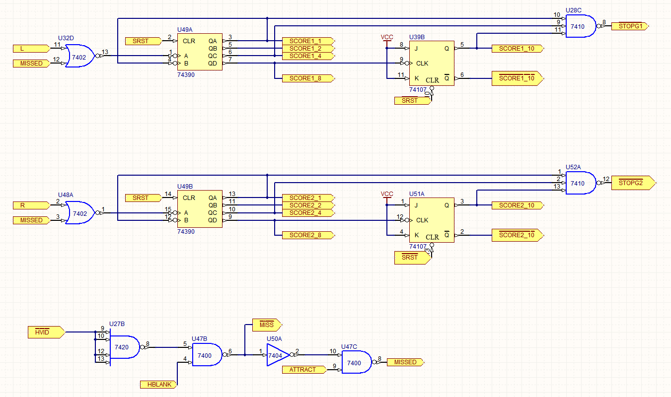
In order to count score and display it, the circuit first checks if the ball's HVID intersected with a HBLANK. If this happens, MISS will be set, and MISSED too in case ATTRACT isn't set.
The MISSED signal is then combined with the L (moving left) and R (moving right) signal to know which of the players was the one that missed and increase the score accordingly.
Each time MISSED is triggered, it clocks the counter and increases score by one. Because QA is connected to B, the counter actually counts only to a decade instead of the full 16 binary value.
The flip-flop after it clocks to remember a decade has passed (the score is over 9), and used afterwards to display the number 1 on screen.
The STOPG signals are for stopping the game once any of the users reaches a score of 15.
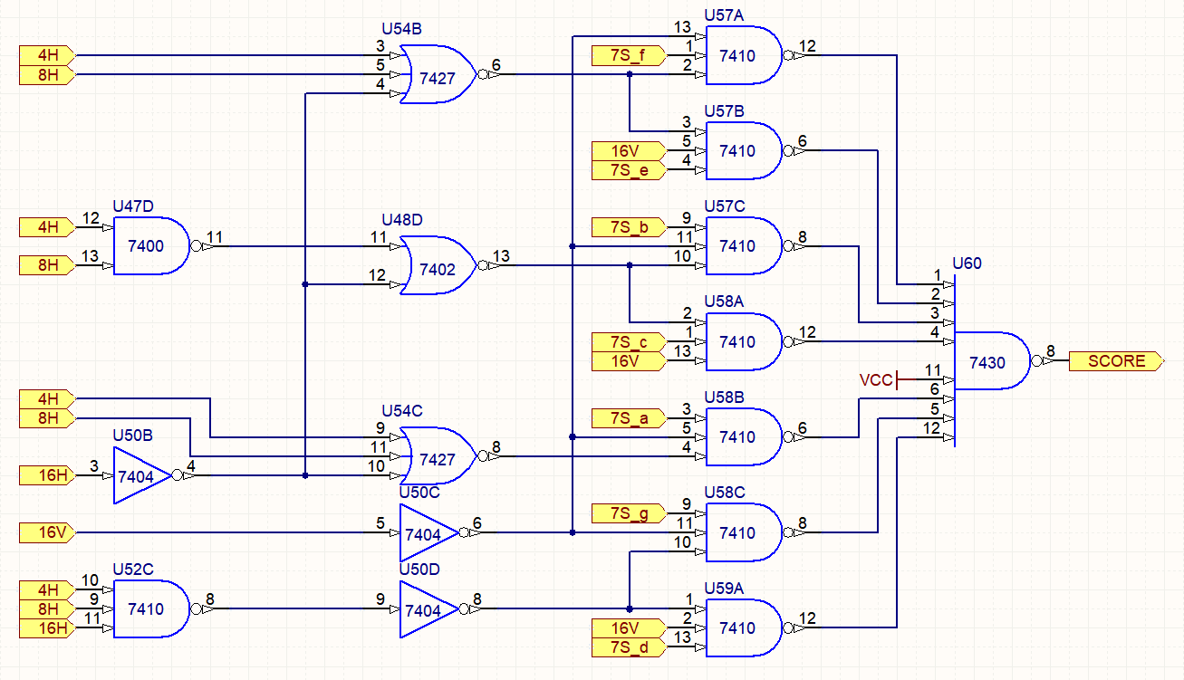
Score Display
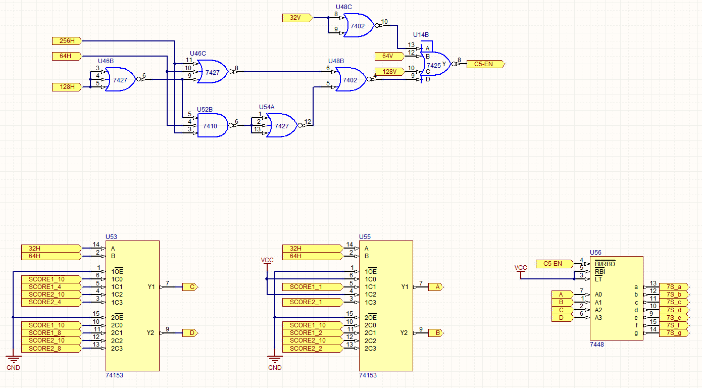
In order to display the score, the score bits of the previous stage are passed through a 4-to-1 multiplexer. This multiplexer uses the 64H and 32H signal to show the numbers in two 64H width window in the screen, each number using 32H space.
This makes it ideal for the 4-to-1 multiplexer, there are 4 windows/numbers which have to be selected in time and each multiplexer has 4 inputs from which to select.
If we observe the 64H and 32H signals closely, we can see that we can locate the first number when 64H is LOW and 32H is LOW, followed by the second number when 64H is LOW and 32H is HIGH, the third when 64H is HIGH and 32H is LOW and so on...
Therefore, we select the signals in the following way:
This data is then fed to a BCD to 7-segment converter in the 7448 IC, which instead of actually going to a 7-segment LED display, it is combined with the rendering signals to display it on screen:
I don't think this part is worth a lot of analysis, but enough to say that each segment of the "supposed" 7-segment display is converted to segments on screen. The horizontal segments are 4V lines thick, while the vertical segments are 4H "pixels" thick. Everything is positioned accordingly.
Dr. Holden explains this beautifully with the following diagram:
Game control
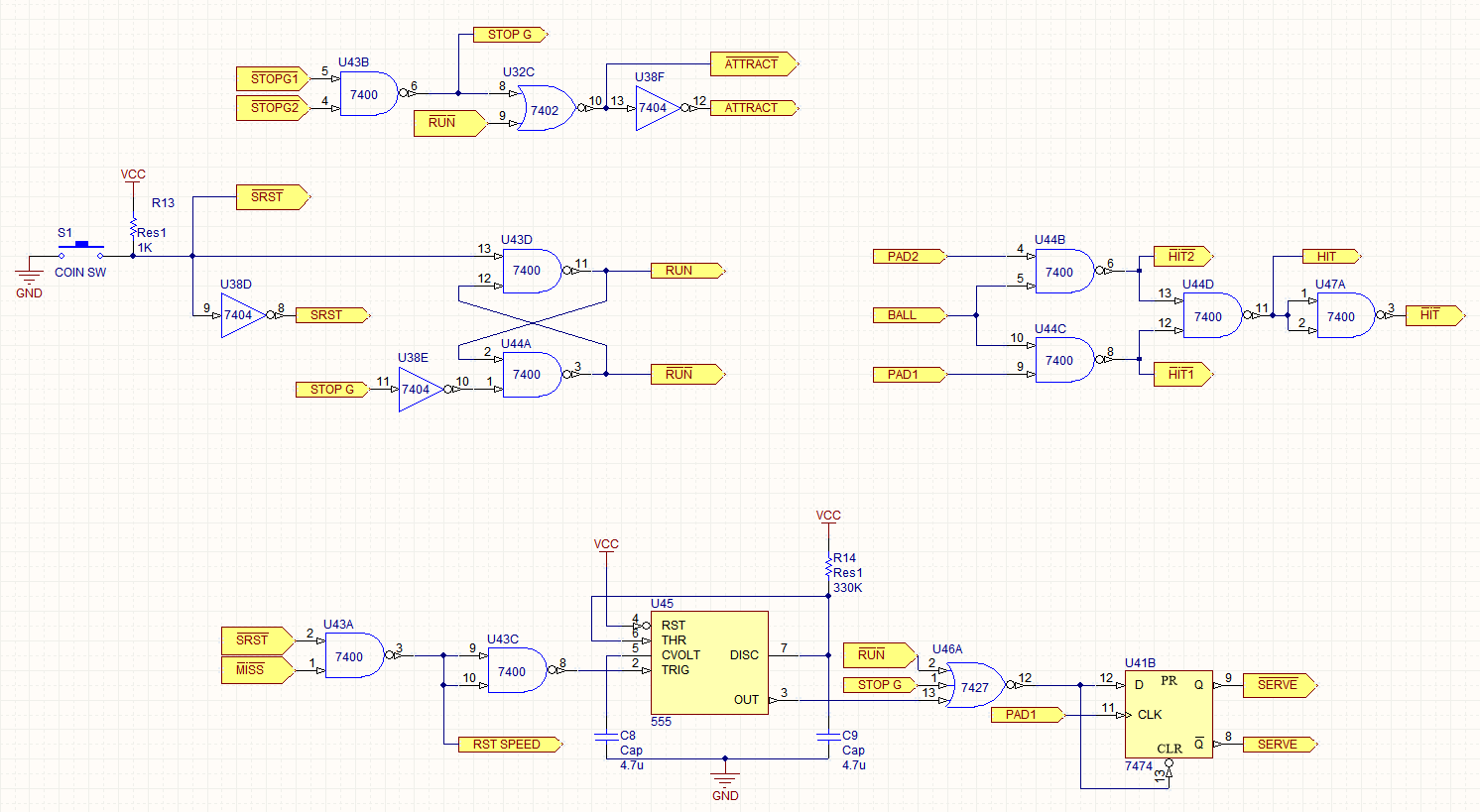
This page of the schematic has more mixed parts of the circuit:
On the top is the logic to stop the game, if any of the players has 15 points, it will trigger the STOPG1 or STOPG2 which in turn will set the STOP G signal, when the game is STOPped and ~RUNning, the game will enter into ATTRACT mode.
On the left side is the coin switch which resets the system SRST and starts a new game throug RUN
On the right side is the part that detects the collision between the ball and the paddles and sets the HIT signal.
On the bottom is the part that handles what happens when the ball was MISSed or the game was reset by a coin. After this, there's a delay before the ball is SERVEd which also depends on the position of PAD1.
SYNC/VIDEO SUM
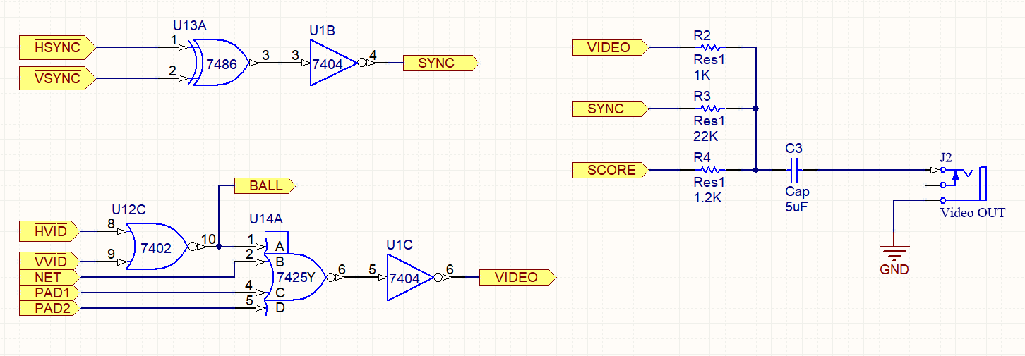
We're finally here! yaaaaaay!
In this part, all the rendering signals are combined to output it into the composite video output though the RCA connector.
Sound
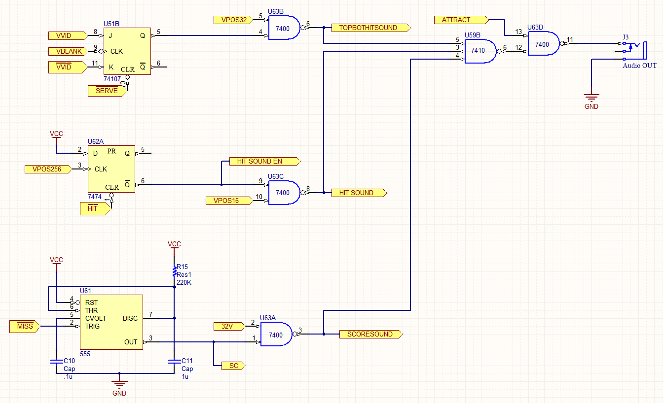
This part handles the sound, I'm getting kinda lazy doing the explanations, but in short the upper part handles the hit sound with the top and bottom edges, the middle handles the hit sound with the paddles and the bottom handles the hit miss sound.
If the game is in ATTRACT mode, the sound is muted.
Part 3: Attempting to do the PCB
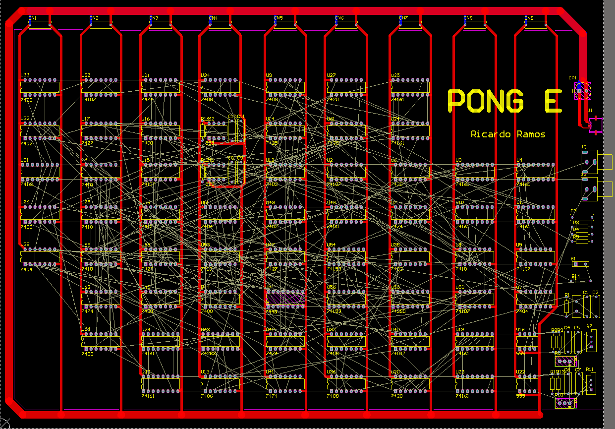
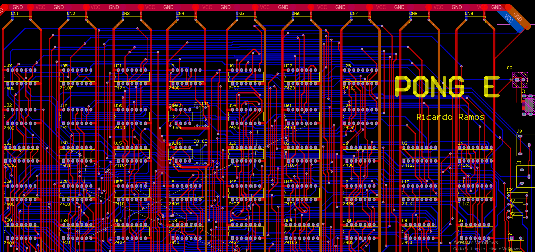
By looking at the pictures in Part 1, I tried to arrange the ICs in a similar fashion, placing them in columns with decoupling capacitors in the top of each colums
At first I thought of making the PCB with the traditional method of etching an FR4 board with Ferric Chloride, so I went to my local store to see if they had that FR4 pieces of that size and unfortunately the biggest chunk I could get my hands on was 30x20cm piece.
This meant everything was going to be tighter in the PCB design (Although after a while I decided not to do it this way as the traces are too thin and too many for the acid to etch properly. It would make it very easy to get disconnected traces in the final result).
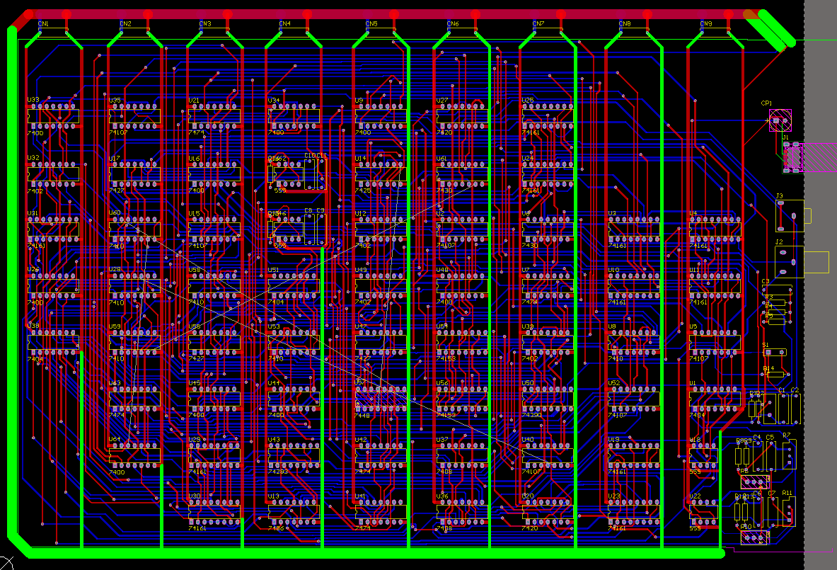
Because there are waaay too many traces in this board (I believe the original board was completely traced by hand!), I just used the auto-router with certain design rules applied. I also had to limit the area on which the auto-router placed the traces by using keepout traces (which is why you see collisions and design rules violations colored in the figure above).
It is usually recommended to not use the autorouter in PCB design, but I think this is an exception and upon closer inspection I think the result isn't too bad.
Part 4: Building the board
Unfortunately a PCB of this size is very expensive to manufature, so I guess I'll just wait to have enough money to continue...